


Featured Blogs
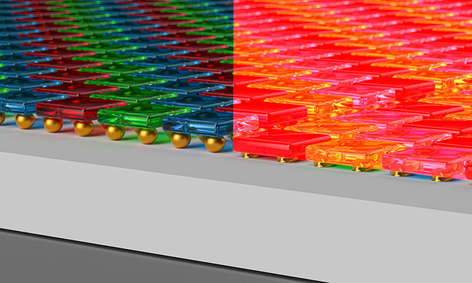
Advanced thermal management
Engineered materials deliver advanced thermal management qualities.
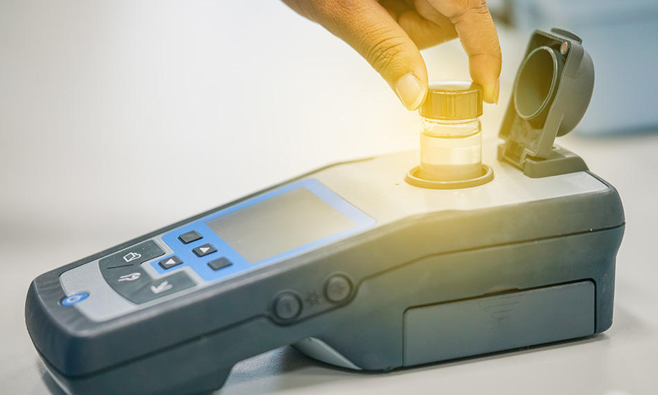
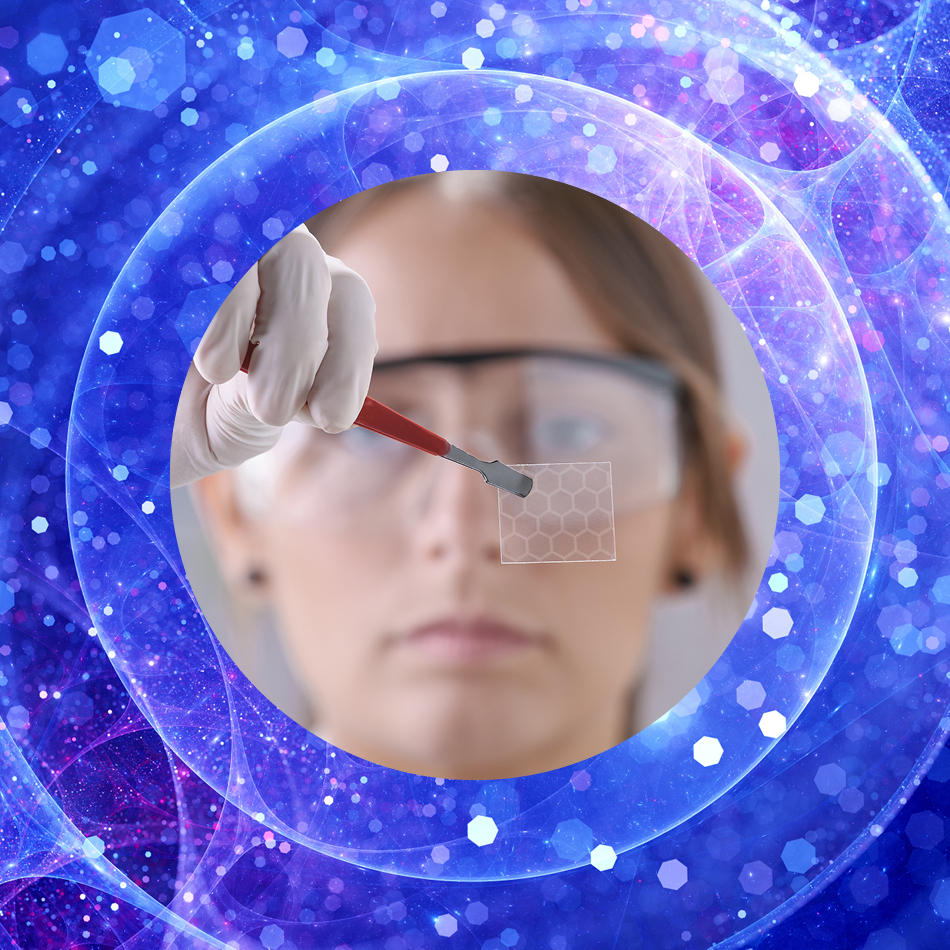
Wearable health monitors
Bio-sensing functions are a cornerstone of modern health monitors.
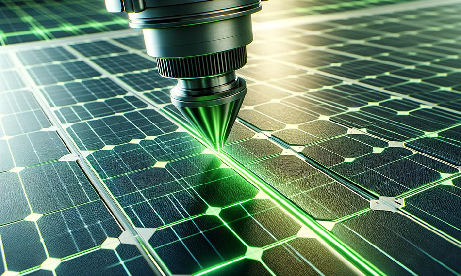
Glasgow : Ultrafast lasers
Coherent Glasgow is the center for our ultrafast laser manufacturing.
Ion implantation foundry services
Integral to semiconductor and engineered materials manufacturing.
Featured Solutions

Featured Event
CYTO 2024
May 4 - 8, 2024
Edinburgh, Scotland
CYTO is the premiere showcase for cytometry-related technologies, featuring some of the top biological, engineering, and environmental companies in the world. Visit CYTO to see the most recent innovations and meet the industry's thought leaders, decision-makers, and scholars.

Featured Products
MATERIALS FOR OPTICS, PHOTONICS, AND ELECTRONICS
Get the highest-quality materials and secure supply chain resiliency from the recognized leader.

Coherent Careers
Our multidisciplinary team of scientists and engineers radically reimagine what’s possible by creating custom solutions for our clients.

Coherent Labs
Solving the most difficult manufacturing challenges with thought leadership and innovative laser systems solutions. Our experts engage customers on over 2,500 projects per year.

Shop Coherent
Online shopping for lasers, optical fibers, power meters and sensors, accessories, and much more on Coherent online has never been easier.